History of Semiconductor Development
The discovery of semiconductors can actually be traced back a long time.
In 1833, British scientist Faraday, the father of electronics, was the first to discover that the resistance of silver sulfide changes with temperature differently from that of ordinary metals, in general, the resistance of metals increases with temperature, but Faraday found that the resistance of silver sulfide material decreases as the temperature rises. This was the first discovery of the semiconductor phenomenon.
Soon after, in 1839, Becquerel in France discovered that the junction formed by contact between a semiconductor and an electrolyte produces a voltage when exposed to light, which is later known as the photovoltaic effect, and this was the second property of the discovered semiconductor. [3]
In 1873, Smith in England discovered the photoconductivity effect of selenium crystalline materials with increased electrical conductivity under light, which is the third property of semiconductors.
In 1874, Braun in Germany observed that the conductivity of certain sulfides is related to the direction of the added electric field, i.e., its conductivity has directionality, and it is conductive when a positive voltage is added at both ends of it; if the voltage polarity is reversed, it is not conductive, which is the rectification effect of semiconductors, and the fourth property unique to semiconductors. In the same year, Schuster also discovered the rectification effect of copper and copper oxide.
Although these four properties of semiconductors were discovered successively before 1880, the term semiconductor was not used for the first time by Kauneberger and Wise until about 1911. And the summary of these four properties of semiconductors was not completed until December 1947 by Bell Laboratories.
In October 2019, an international team of researchers claimed that the new technique could obtain up to seven parameters per test light intensity compared to only three parameters obtained in conventional Hall measurements: including electron and hole mobility; loadon density in light, recombination lifetime, and diffusion length for electron, hole, and bipolar types.
Semiconductor Applications
Semiconductors are used in integrated circuits, consumer electronics, communication systems, photovoltaic power generation, lighting applications, high-power power conversion, and other applications.
Photovoltaic Applications
The photovoltaic effect of semiconductor materials is the basic principle of solar cell operation. At this stage, photovoltaic applications of semiconductor materials have become a major hit, and is currently the fastest growing and best developed clean energy market in the world. Solar cells are mainly made of semiconductor materials, the main criterion for judging the merits of solar cells is the photoelectric conversion rate, the higher the photoelectric conversion rate, the higher the efficiency of solar cells. Depending on the semiconductor material used, solar cells are classified as crystalline silicon solar cells, thin film cells, and III-V compound cells.
Lighting applications
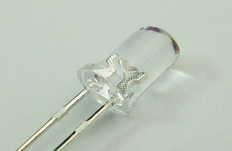
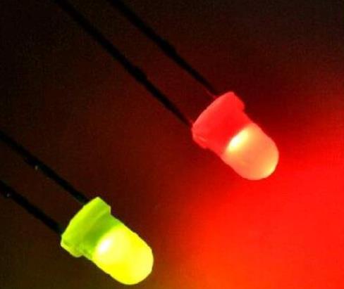
LED is a semiconductor light-emitting diode built on a semiconductor transistor , the use of LED technology semiconductor light source is small, can achieve flat packaging, low heat generation, energy efficient, long product life, fast response time, and green, non-polluting, can also be developed into thin and short products , once introduced , it has rapidly become popular, a new generation of high-quality lighting source, has been widely used In our life. Such as traffic lights, backlighting of electronic products, city night landscape beautification light source, indoor lighting and other fields, have applications.
High-power power conversion
AC and DC power conversion is very important for the use of electrical appliances, is the necessary protection of electrical appliances. This requires the use of power conversion devices. The high breakdown voltage strength, wide band width and high thermal conductivity of silicon carbide make SiC semiconductor devices very suitable for applications with high power density and switching frequency, of which power conversion devices are one. The high temperature, high voltage, and high frequency performance of SiC components has led to a wide range of applications such as deep well drilling, inverters in power generation, energy converters in electric hybrid vehicles, and traction power conversion in light rail trains.
Due to SiC’s own advantages and the current industry need for lightweight, high conversion efficiency semiconductor materials, SiC will replace Si as the most widely used semiconductor material.

