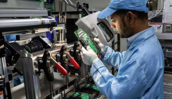
Recently, the media said that India is discussing with China’s Taiwan-based foundry UMC to build a joint wafer fab matters, the two sides are likely to build a joint fab worth about $ 7.5 billion. In recent years, India has achieved rapid development in the field of electronics manufacturing, mainly cell phone foundry, Samsung, Xiaomi, Huawei, OPPO, vivo as the representative of cell phone manufacturers have set up factories in India production. India Electronics Industry Association (Elcina) December 30, 2020, said that India’s electronics manufacturing industry is expected to grow sixfold in 2025 to $152 billion. This also makes the importance of semiconductor technology increasingly prominent, the Indian government began to focus on the development of semiconductor industry.
However, India’s local development of semiconductor industry has many advantages at the same time, there are also many “hard”, which makes China and Taiwan manufacturers for this cooperation to remain hesitant. If India’s semiconductor industry wants to rise, the choice of foundry road may not be the expedient solution.
Open market for technology
In March this year, India announced a $1 billion cash subsidy for each chip company going to India to vigorously develop India’s indigenous chip manufacturing industry. Therefore, India this time also hopes to rely on its greater government incentives to cooperate with external semiconductor companies. It is understood that India’s ZX eyes on TSMC. However, sources say that TSMC is likely to turn down the invitation, considering its more work to expand and increase production everywhere. For its part, UMC may value the Indian government’s incentives due to its lower spending budget, thinner margins, and the relatively old technology required in India. The cooperation between the two sides may be the joint construction of a wafer fab worth about $7.5 billion, and the local government in India may pay half of the cost for this.
In the outside world, although the Indian electronic information industry as a whole is relatively backward, but the development of semiconductor still has some advantages.
One, India is one of the QQ range of ZD electronics market. In the 1990s, the Indian government has issued a document to support the software industry, the introduction of “zero tax” policy, software and service companies to give bank loans “priority”, triggered a revolution in the Indian software industry. This has also greatly contributed to the development of the Indian semiconductor industry. According to the Indian Electronics and Semiconductor Association (IESA), by 2025, the Indian semiconductor components market is expected to be worth $32.35 billion, growing at a combined annual growth rate of 10.1% between 2018 and 2025.
Second, the Indian government realized the importance of the semiconductor industry early on and provided a lot of policy support. Since 2005, India has decided to vigorously develop the chip manufacturing industry. 2012, the Indian government announced a policy covering various sectors of the electronics industry, planning the establishment of 200 electronic manufacturing clusters (EMC). Subsequently, India will improve the special incentive program and electronic development fund, etc., the allocation of the incentive program increased to $ 111 million.
Industry ZJ with the “China Electronics News” reporter said, India and China Taiwan enterprises, can be simply understood as an open market in exchange for technology.
Infrastructure and talent are the shortcomings
Despite its many advantages, in terms of wafer foundry, India’s development has not been smooth. It is understood that this has been India’s third attempt in 20 years to enter the foundry business, each previous failure has led to considerable losses. And this cooperation is also very unlucky, first by TSMC politely rejected, and UMC’s deal can also be described as a series of twists and turns. India’s development of semiconductor weaknesses in the end where?
It is understood that the development of the semiconductor industry in India has two major problems. First, India’s local infrastructure is very backward, road transport, water, electricity, logistics and other aspects are difficult to guarantee, and the foundry industry needs strong infrastructure to support, otherwise it is difficult to maintain.
Industry ZJ to “China Electronics News” reporter said, in general, a foundry from construction to production, the entire return cycle in more than ten years, if also bear the risk of local supply in water, electricity, the return cycle will be longer. Any wafer foundry, when investing in new plants to consider the cost and economic benefits, which is the basic elements of business development. Therefore, the lack of infrastructure in India, for the foundry is often a hard wound, which can cause significant economic losses.
In addition, despite India’s talent training SJLX in IT, the brain drain problem is very serious, making India’s own high-tech talent is very scarce. A study has found that India is the country with the Z most QQ brain drain. Because of the low salary level and poor working environment in India itself, it makes India’s high-tech talents flow to Europe and America. According to statistics, at least two-thirds of Indian graduates will choose to leave India every year, and 38% will stay in the United States. Although the Indian government has set up some financial aid programs and measures to retain talents, most IT graduates still go to the U.S. Silicon Valley before and after, which shows that the brain drain has become a ZD obstacle to the development of India’s IT industry.
In addition, although India’s local labor force is cheap, but it does not mean that the employment cost is low. In addition to the cost of employment, the cost of wages, but also take into account efficiency and bad rate and other factors. And in these two points, Indian workers do not take advantage of.
The development of packaging industry may be more appropriate
Some industry analysts say that this time, India and UMC to build a foundry, it is likely to be the same as the previous, to “abort” and end. However, the Indian semiconductor is really no way out? Not so, if the Indian semiconductor to achieve development, perhaps another way to develop packaging technology is more appropriate.
Throughout the development of Indian semiconductor road, and the development of Chinese semiconductor has many similarities. It is understood that China’s semiconductor in the beginning of development, also encountered many similar problems. For example, Z early China’s infrastructure is not perfect, the relevant talent training mechanism is not perfect. The key point is that China has chosen the right development path for packaging.
Industry ZJ to “China Electronics News” reporter, China’s semiconductor in packaging is more prominent, but also thanks to a unique advantage – labor-intensive and relatively cheap, and packaging is an industry that requires a lot of labor to hold up, which also makes China’s development in packaging is very rapid, greatly promoting the relevant technology innovation. With the advent of the post-Moore era, packaging technology is also gaining more and more attention, and is even expected to become the key to drive a qualitative leap in China’s semiconductor industry in the future.
In addition, to do a good job in the foundry industry is not easy, not only for India, for countries around the world is a problem. It is understood that QQ has more than 170 semiconductor manufacturing plants cost more than $ 1 billion, if you want to be among the advanced process, the cost is even higher.
Therefore, for the situation with the former China is somewhat similar to India, than the wafer foundry, the expansion of the packaging industry may be more suitable.