Recently, Intel held a process technology and packaging technology online conference. At the meeting, Intel CEO Pat Kissinger said that Intel is through the semiconductor process technology and packaging technology to achieve technological innovation, and announced the most detailed process technology and packaging technology development route ever, and said that in 2025 “to recover lost ground”, to regain the dominant position in the chip market.
Why Intel can have such confidence this time? The latest release of the future technology route can really help in the previous ill-fated Intel, and make it revitalized to start again?
Various challenges sounded the alarm for Intel
As the world’s largest manufacturer of personal computer parts and CPU, Intel has dominated the market for decades. However, in the past decade, Intel began to face unprecedented competitive pressure and challenges. First, it was completely defeated by arm in the mobile market, then it was overtaken by NVIDIA in the field of artificial intelligence, and was counterattacked by TSMC in manufacturing.
In terms of chip manufacturing process, Intel has also encountered many difficulties. In addition to a small increase in frequency and small specification changes, Intel has not made a great breakthrough in the progress of process upgrading in recent years. First, several major delays in the 10nm process technology completely disrupted the development rhythm of Intel.
Later, Intel 7Nm process chip, which was highly expected, also entered the dilemma of “dystocia”, which directly led to Intel’s big customer Apple choosing to “go its separate ways”, ending 15 years of cooperation, and choosing to introduce self-developed arm architecture chip into the product.
During this period, TSMC, Intel’s largest competitor, has had a smooth journey. TSMC’s 5nm process chips have achieved mass production. In addition, TSMC is still promoting the mass production of more advanced 4nm and 3nm processes, and will start the risk trial production of 4nm process in the third quarter of this year.
All kinds of competitive pressures are always ringing alarm bells for Intel, therefore, in order to reverse the decline of Intel in the semiconductor industry competition, Pat Kissinger took office and proposed the IDM2.0 plan, the future of Intel’s manufacturing changes to: “Intel factory + third-party capacity + foundry services” combination.
There are several key information: First, the investment of $ 20 billion in the United States to build two wafer fabs; second, the full-scale external foundry services to the United States and European factories as a base to grab TSMC business; third, to expand the volume of outsourcing orders; fourth, the joint research and development of the next generation of logic chip packaging technology with IBM.
It can be seen that, as part of the IDM2.0 strategy, Intel is accelerating its own development pace through semiconductor process technology and packaging technology, which is also the key to Intel’s determination to return to the top of the industry by 2025.
The most detailed technology development route ever
In this conference, Intel announced the most detailed process technology and packaging technology development route ever, and both process technology, or packaging technology, can be described as a highlight, breaking many of the original model and concept, so that people see the new side of Intel.
At the press conference, Pat Kissinger introduced, for decades, the name of the chip process node to the gate length of the transistor to name. However, today, the entire industry for the chip process node naming also began to diversify, these diverse programs no longer refer to any specific metrics, nor can reflect how to achieve a balance of energy efficiency and performance.
Therefore, Intel from the performance, power consumption and area and other aspects of a comprehensive consideration of the chip process process using a new naming system. Previously, the media said that Intel intends to spend $ 30 billion to acquire the foundry core, and this may be closely related to Intel’s new process development line.
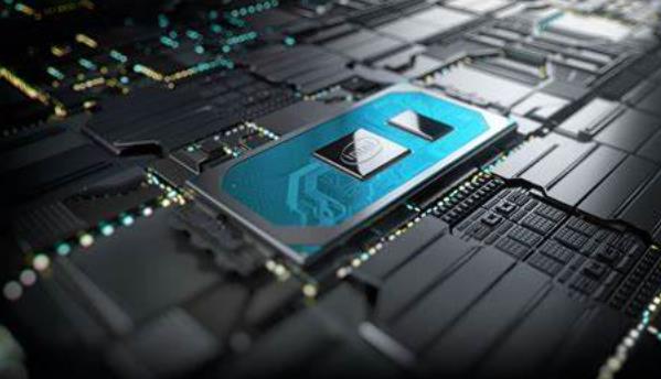
At the press conference, Intel announced the technology roadmap for the chip manufacturing process in the next five years and adopted a new naming system, namely Intel 7 (previously known as 10 nm enhanced superfin), Intel 4 (previously known as Intel 7 nm), Intel 3 and Intel 20A. Among them, Intel 7 process has the best FinFET transistor, and the performance per watt will be improved by about 10% ~ 15% compared with Intel 10nm superfin; In Intel 4, EUV lithography technology will be fully adopted, and ultra short wavelength lithography can be used to print very small patterns; In the Intel 3 process, the performance per watt will be improved by about 18% compared with Intel 4.

After the Intel 3 process, the chip manufacturing process will be closer and closer to the 1 nm node and enter the smaller Amy era. Therefore, for the process after Intel 3, Intel has also changed its naming method and named it Intel 20a, which will open the Amy era with two breakthrough technologies of ribbonfet and powervia. Song Jiqiang, vice president of Intel Research Institute and President of Intel China Research Institute, said that the reason why Intel 3 does not directly become Intel 2, but Intel 20a, is a new naming rule adopted by Intel in order to grasp the future technology